所屬科目:研究所、轉學考(插大)◆電子學
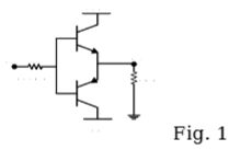
1. The BJTs in Fig. 1 have β = 100. Find VB and VE for Vi = +3Vand -10V, respectively. (16%, each sub-question takes 4%)
(a) indicate the operating region (3%), and
(b) calculate the base current IB, collector current IC and Vo (12%,Each sub-question takes 4%)
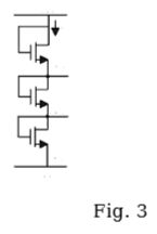
3.For the voltage divider with I = 90 μA, shown in Fig. 3, e MOSFET has VT = 1V, μnCox = 20 μA/V2, and neglect the effectof ro. Design the W/L ratio of each Q1, Q2, and Q3 MOSFETs suchthat the source voltage V1 of the transistor Q1 is +1 V and sourcevoltage V2 of the transistor Q2 is -1 V. (18%, Each sub-questiontakes 6 %)
(a) Find the values of RE and RC, such that IE = 2 mA and VBC =4.5 V. (12%, each sub-question takes 6 %)
(b) Find the values of IE and VBC when RE = 3.9 kΩ and RC = 2.2kΩ. (12%, Each sub-question takes 6 %)
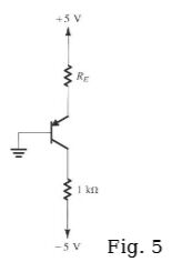
5. Select a value for “RE” in Fig. 5 so that the transistor saturateswith a forced β of 30. Assume VEB = 0.7 V and VEC,sat = 0.2 V. (12%)
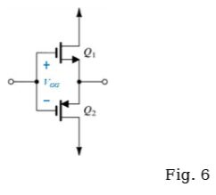
6. The design of a class AB MOS output stage, as shown in Fig. 6,is being considered, where each transistor has |Vt| = 1 V and μCoxW/L = 300 mA/V2.What value of gate-to-gate bias voltage “VGG” is required suchthat the incremental output resistance of the equivalent circuitin the quiescent state is 25 Ω? (15%)
 阿摩線上測驗
登入